Working With I/O Registers
AVR I/O Registers are a set of 64 bytes that occupy the space in Data Memory immediately following the 32 general purpose working registers. Thus, they are contained in the Data Memory addresses 0x20 through 0x5F. The I/O Registers contain all of the PORT, PIN and DDR registers used to control the microcontroller's pins, as well as some of the more important control registers.
Because they are used so often, the AVR has a set of special instructions specifically for manipulating and checking these registers, shown in the table below.
| Mnemonic | Description |
|---|---|
| in | in from I/O location |
| out | out from I/O location |
| cbi | clear bit in I/O register |
| sbi | set bit in I/O register |
| sbic | skip if bit in I/O register cleared |
| sbis | skip if bit in I/O register set |
Any of the 64 I/O Registers can be loaded into any of the 32 working registers using the in instruction.
	in	r0,DDRB			; load DDRB into r0
	in	r15,TCNT0		; load TCNT0 into r15
	in	r31,MCUCR		; load MCUCR into r31
Similarly, any of the 32 working registers can be written to the any of the 64 I/O Registers using the out instruction.
	out	DDRB,r0			; load r0 into DDRB
	out	TCNT0,r15		; load r15 into TCNT0
	out	MCUCR,r31		; load r31 into MCUCR
Since the Status Register is part of the I/O Registers, in and out can be used to preserve its contents after a subroutine call. For example
	in	r0,SREG			; load SREG into r0
	push	r0			; push r0 to the stack

	rcall	mySubroutine		; call subroutine

	pop	r0			; pop value from stack to r0
	out	SREG,r0			; restore SREG
The instructions sbi and cbi allow you to set or clear a bit in an I/O Register. These instructions do not work with all 64 I/O Registers - only the first 32. However all of the PORT, PIN and DDR registers are contained in the first 32 memory locations, making this instruction ideal for setting outputs to pins. For example, lighting an LED on PINB0 can be done simply as
	sbi	DDRB,PINB0		; set PINB0 to ourput
	sbi	PORTB,PINB0		; set PINB0 high
Note that sbi and cbi expect a pin number rather than a mask. This means only one bit may be set at a time. Thus, if you need to set severl bits it may be more efficient to use in and out.
	sbi	PORTB,PINB0		; set PINB0 high
	sbi	PORTB,PINB1		; set PINB1 high
	sbi	PORTB,PINB3		; set PINB3 high
	sbi	PORTB,PINB5		; set PINB5 high

	; alternatively

	in	r16,PORTB
	ori	r16,(1<<PINB0)|(1<<PINB1)|(1<<PINB3)|(1<<PINB5)
	out	PORTB,r16
The instructions sbis and sbic allow you to "skip" an instruction based on a condition in an I/O Register. As with sbi and cbi, these instructions only work with the first 32 I/O Registers.
sbis and sbic are useful for checking a condition on an external pin. For example, a loop which waits until PINB0 is cleared by (e.g. by a button) could be written as
wait:	sbic	PINB,PINB0		; skip if PINB0 is low
	rjmp	wait			; repeat loop
I/O Addresses vs. Data Memory Addresses
If you look in the datasheet, you will notice that two addresses are given for I/O Registers. For example, the Status Register is shown with the addresses 0x3F and in parentheses 0x5F.
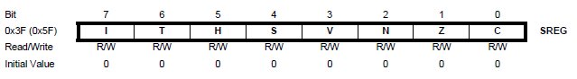
The first address is the I/O address, and the second is the Data Memory address. In order to efficiently map I/O Registers with the minimum number of bits for the instructions above, the I/O Registers are renumbered, with Data Memory address 0x20 becoming I/O address 0x00. Thus the first 32 I/O Registers can be represented by only 5-bits and the entire 64 can be represented by 6. There are only so many bits available in an instruction's opcode and this compromise had to be made by the chip's designers. It at least allows easy access to some of the I/O Registers, but not all.
Note: I/O Addresses are only used for the instructions shown above. For the other instructions shown later, data memory addresses must be used instead.
In Atmel include files, the I/O Registers that can be accessed by the instructions above are defined by their I/O addresses, so no conversion is necessary. Be careful when using other memory access instructions though since using them as is may produce undesired results.